
Photodiode test
Focus on semiconductor electrical performance testing
Position:Home > Solutions > Semiconductor discrete devices
Overview
Diode is a semiconductor device that converts light into current . There is an intrinsic layer between the p (positive) and n (negative) layers. The photodiode accepts the light energy as input to generate electric current. Photodiodes are also known as photodetectors, photosensors or photodetectors, common are photodiodes (PIN), avalanche photodiode (APD), single photon avalanche diode (SPAD) , silicon photomultiplier (SiPM / MPPC).
Photodiode (PIN) also known as PIN junction diode, where a layer of I-type semiconductor is low in the middle of the photodiode PN junction , can increase the width of the depletion area,reduce the impact of diffusion movement and improve the response speed. Due to the low doping concentration of this incorporation layer
, almost intrinsic semiconductor, it's called I-layer, so this structure becomes PIN photodiode;
Avalanche photodiode(APD) is a photodiode with an internal gain, the principle similar to a photomultiplier tube. After add a high reverse bias voltage (generally 100-200V in silicon materials), internal current gain of approximately 100 can be obtained in the APD by using the ionization collision (avalanche breakdown) effect;
Single photon avalanche diode(SPAD) is a photoelectric detection avalanche diode with single photon detection capability operating in APD (Avalanche Photon Diode) in Geiger mode. Applied to Raman spectroscopy, positron emission tomography, and fluorescence lifetime imaging areas ;
Silicon photomultiplier (SiPM) is a kind of working on the avalanche breakdown voltage and has the avalanche quenching mechanism of avalanche photodiode array in parallel, with excellent photon number resolution and single photon detection sensitivity of silicon low light detector, with high gain, high sensitivity , low bias voltage, not sensitive to magnetic field, compact structure.

PIN photodiodes have no multiplier effect and are often applied in the short-range detection field. APD avalanche photodiode technology is relatively mature and is the most widely used photodetector. Thetypical gain of APD is currently 10-100 times, light source needs to significantly increase to ensure that the APD has a signal during long-distance test, SPAD single photon avalanche diode and SiPM / MPPC silicon photomultiplier exist mainly to solve the gain capability and the implementation of large-size arrays:
1) SPAD or SiPM / MPPC is an APD working in Geiger mode, which can obtain a gain of tens to thousands of times, but the system and circuit costs are high;
2) SiPM / MPPC is an array form of multiple SPAD, which can obtain higher detectable range and use with array light source through multiple SPAD, so it's easier to integrate CMOS technology and has the cost advantage of mass production scale. In addition, as SiPM operating voltage is mostly lower than 30V, no need high voltage system, easy to integrate with mainstream electronic systems, the internal million- level gain also makes SiPM requirements for the back- end readout circuit simpler. At present, SiPM is widely used in medical instruments, laser detection and measurement (LiDAR), precision analysis,
radiation monitoring, safety detection and other fields, with the continuous development of SiPM, it will expand to more fields.
Photodetector Photoelectric Test
Photodetectors generally need to test the wafer first,then perform a second test on the device after packaging to complete the final characteristic analysis and sorting operation; when the photodetector is working, it needs to apply a reverse bias voltage to pull the light out. The generated electron- hole pairs are injected to complete the photogenerated carrier.So photodetectors usually work in the reverse state; during testing, more attention is paid to parameters such as dark current, reverse breakdown voltage, junction capacitance, responsivity, and crosstalk.
Use The Digital Sourcemeasure Meter
Photoelectric performance characterization of photodetectors
One of the best tools for the characterization of photoelectric performance parameters is the digital source measure meter (SMU). Digital source measure meter as independent voltage source or current source, can output constant voltage, constant current, or pulse signal, can also be as a instrument for voltage or currentmeasurement; support Trig trigger, multiple instruments linkage work; for photoelectric detector single sample test and multiple sample verification test, a complete test scheme can be directly built through a single digital source measure meter, multiple digital source measure meter or card source measure meter.
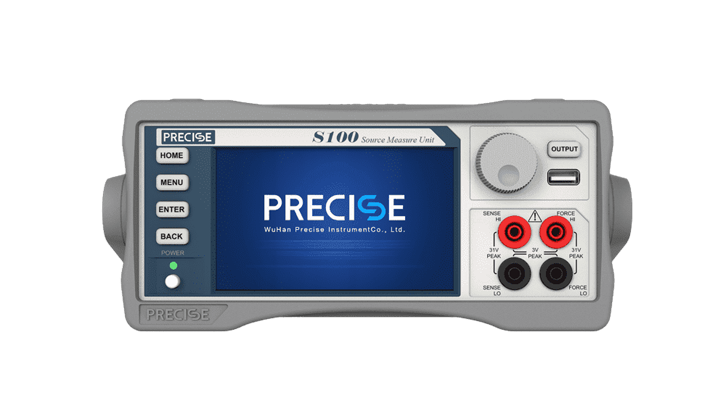
PRECISE Digital Source measure Meter
Build the photoelectric test scheme of the photoelectric detector
Dark current
Dark current is the current formed by PIN / APD tube without illumination; it's essentially generated by the structural properties of PIN / APD itself, which is usually below μA grade.
Using the S series or P series source measure meter, the minimum current of S series source measure meter is
100 pA, and the minimum current of P series source measure meter is 10 pA.
Testing circuits

IV curve of dark current
When measuring the low level current(< 1 μA), the triple coaxial connectors and triple coaxial cables can be used. The three coaxial cable is composed of the inner core (the corresponding connector is the central contact), the protective layer (the corresponding connector is the middle cylindrical contact), and the outer skin shielding layer. In the test circuit of the protection end of the source measure meter, as there is equipotential between the three coaxial protection layer and the inner core , there will be no leakage current generation , which can improve the accuracy of lowcurrent test.

Interfaces of source measure meter

Triaxial Adapter
Breakdown reverse voltage
When the applied reverse voltage exceeds a certain value, the reverse current will suddenly increase, this phenomenon is called electric breakdown. The critical voltage that
causes electrical breakdown is called the diode reverse breakdown voltage.
According to the different specifications of the device, the voltage resistance index is not consistent, and the instrument required for the test is also different. It is recommended to use S series desktop source measure meter or P series pulse source measure meter below 300V, the maximum voltage is 300V, the breakdown voltage above 300V is recommended, and the maximum voltage is 3500V.

Connection circuits

Reverse breakdown voltage IV curve
C-V Test
The junction capacitance is an important property of the photodiode and has a great influence on its bandwidth and response. It should be noted that the diode with a large PN junction area has a larger junction volume and also has a larger charging capacitor. In reverse bias application, increasing the depletion zone width of the junction effectively reduces the junction capacitance and increases the response speed. The photodiode C-V test scheme consists of S series source measure meter, LCR, test clamp box and upper computer software. The test circuit and curve diagram are shown as below.
CV testing connection circuits

CV curve
Responsivity
The responsivity of the photodiode is defined as the ratio of the generated photocurrent (IP) to the incident light power (Pin), at the specified wavelength and reverse bias, usually in A / W. The responsivity is related to the magnitude of the quantum efficiency, which is the external embodiment of the quantum efficiency, and the responsivity is R=IP / Pin. Using the S series or P series source measure meter, the minimum current of S series source measure meter is 100 pA, and the minimum current of P series sourcemeasure meter is 10 pA.
Optical Crosstalk Test (Crosstalk)
In the lidar field the number of photodetectors used in lidar products with different lines is different, and the interval between photodetectors is very small. In the process of use, there will be mutual optical crosstalk at the same time, and the existence of optical crosstalk will seriously affect the performance of lidar.
Optical crosstalk takes two forms: the light incident at a large angle above the array enters the adjacent photodetector and is absorbed before being fully absorbed by the photodetector; second, a part of the large-angle incident light is not incident to the photosensitive area, but is incident to the interconnecting layer between the photodetectors and is reflected into the photosensitive area of the adjacent device.
Array detector optical crosstalk test is mainly for array DC crosstalk test, which refers to the maximum value of the ratio of the photocurrent of the light unit to any adjacent unit photocurrent in the array diode under the specified reverse bias, wavelength and optical power.
S/P Series Test Solution
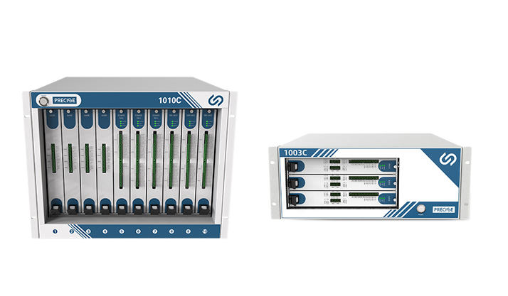
CS Series Multi-channel Test Solution
The test by the trial S series, P series, or CS series multi-channel testing scheme is recommended.
This scheme is mainly composed of CS1003C / CS1010C host and CS100 / CS400 subcard, which has the characteristics of high channel density, strong synchronous trigger function and high multi-device combination efficiency.
CS1003C / CS1010C: Using custom frame, backplane bus bandwidth up to 3 Gbps, support 16 trigger bus, to meet the needs of high speed communication of multi-card equipment, CS1003C has a slot for up to 3 subcards, CS1010C has a slot for up to 10 subcards.

CS100 subcard: single card single channel subcard with four quadrant working capacity, maximum voltage of 300V, minimum current of 100 pA, output accuracy of 0.1%, maximum power of 30W; up to 10 test channels.
CS400 subcard: a single card four-channel word card with 4 channels, the maximum voltage of 10V, the maximum current of 200 mA , output accuracy of 0.1%, single channel
maximum power of 2W; can build 40 with CS1010 host test channels.
Optical Coupling (OC) Electrical Performance Test Solution
Optical coupler (optical coupler, English abbreviation OC) is also known as photoelectric separator or photoelectric coupler, referred to as photocoupler. It is a device that transmits electrical signals with light as the medium. It is generally composed of three parts: light transmission, light reception and signal amplification. Theinput electrical signal drives a light- emitting diode (LED), causing it to emit a certain wavelength of light, which is received by the optical detector to generate a photocurrent, which is further amplified and output. This completes the conversion of electricity one light one electricity, thus playing the role of input, output and isolation.
Because the input and output of optical coupler are isolated from each other, the transmission of electrical signals is unidirectional, so it has good electrical insulation ability and anti-interference ability, so it is widely used in various circuits. At present, it has become one of the most diverse and widely used photoelectric devices.
For optical coupling devices, the main electrical performance characterization parameters are: forward voltage VF, reverse current IR, input capacitance CIN, emitter- collector breakdown voltage BVcEo, current conversion ratio CTR, etc.
Direct Voltage VF
VF refers to the pressure drop of the LED itself at a given operating current. Common low-power LEDs usually test the forward operating voltage with the mA current. The Perth S series or P series source measure meter is recommended during testing.
Vf testing circuits
Reverse Leakage Current IR
Usually the reverse current flowing through the photodiode at the maximum reverse voltage, usually the reverse leakage currentis at the nA level. The test S series or P series sourcemeasure meter has the ability to work infour quadrants, it can output negative voltage without adjusting the circuit. When measuring low level current (<1 μ A), three coaxial connectors and triple coaxial cables are recommended.
Embitter-collector Breakdown Voltage BVcEO
It refers to the VcEo value when the output current starts to increase under the condition of open circuit. According to the different specifications of the device, the voltage resistance index is not consistent, and the instrument required for the test is also different. It is recommended to use S series desktop source measure meter or P series pulse source measure meter below 300V, the maximum voltage is 300V, the
breakdown voltage above 300V is recommended , and the maximum voltage is 3500V.
BVceo testing circuits
Current Transfer Ratio CTR
Current Transfer ratio CTR (Current Transfer Ratio), when the operating voltage of the output tube is the specified value, the ratio of the output current and the forward current of the light-emitting diode is the current conversion ratio CTR. The Perth S series or P series source measure meter is recommended during testing.
Isolation Voltage
Insulation voltage resistance between the input and output ends of the optical coupler. Generally, the isolation voltage is high, and a large voltage equipment is required for testing. The E-series source measure meter is recommended, and the maximum voltage is 3500V.

isolation voltage testing circuits
Isolated Capacitance Cf
The isolated capacitance Cr refers to the capacitance value between the input and output terminals of the photocoupled device.
The test scheme consists of S series source measure meter, digital bridge, test clamp box and upper computer software. The test circuit and curve diagram are shown below.
isolation capacitor testing circuits

Cf curve
Conclusion
Wuhan PERCISE instrument has been focused on semiconductor electric performance test instrument development, based on the core algorithm and system integration technology platform advantages, the first independent research and development of high precision digital source measure meter, pulse source measure meter, narrow pulse source measure meter, integrated card source measure meter products are widely used in the analysis of semiconductor device material and testing field. According to the needs of users,we offer with the most efficient, cost -effective semiconductor test solutions.


 Email
Email
 Contact
 Inquiry
 Home
Home
