
How To Quickly And Accurately Analyze Triode BJT Characteristics
Focus on semiconductor electrical performance testing
Position:Home > Solutions > Semiconductor discrete devices
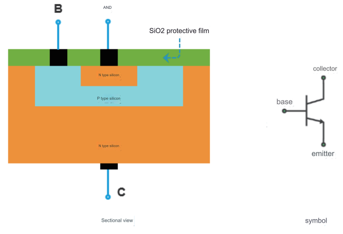
Bipolar junction transistor-BJT is one of the basic components of semiconductors.It has the function of current amplification and is the core component of electronic circuits.The BJT is made on a semiconductor substrate with two PN junctions that are very close to each other.The two PN junctions divide the whole semiconductor into three parts.The middle part is the base region,and the two sides are the emitter region and the collector region.

BJT characteristics that are often concerned in designing circuits include current amplification factor β,inter-electrode reverse current ICBO,ICEO,collector maximum allowable current ICM,reverse breakdown voltage VEBO,VCBO,VCEO,and input and output characteristics of bjt.
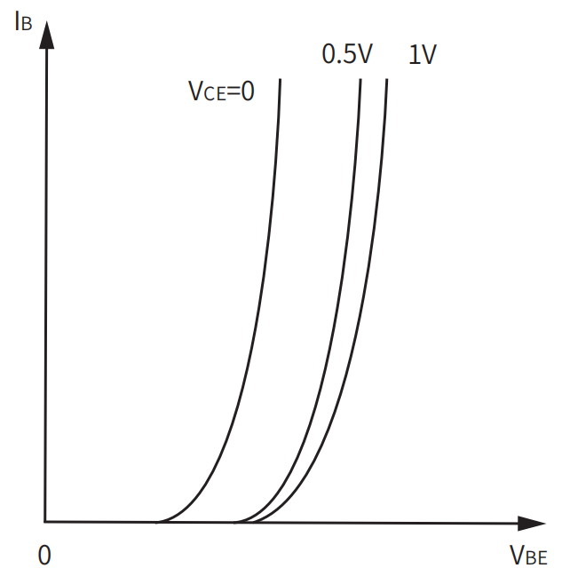
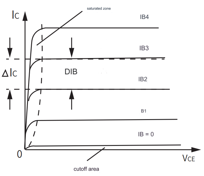
BJT input and output characteristics curve reflects the relationship between the voltage and current of each electrode of the bjt.It is used to describe the operating characteristic curve of the bjt.The commonly used bjt characteristic curves include the input characteristic curve and the output characteristic curve:
The input characteristics of bjt curve indicates that when the voltage Vce between the E pole and the C pole remains unchanged,the relationship between the input current (ie, the base current IB) and the input voltage (ie, the voltage between the base and the emitter VBE) ; When VCE = 0,it is equivalent to a short circuit between the collector and the emitter, that is,the emitter junction and the collector junction are connected in parallel. Therefore, the input characteristics of bjt curve is similar to the volt-ampere characteristics of the PN junction,and has an exponential relationship.When Vce increases,the curve will shift to the right.For low-power transistors,an input characteristic curve with VcE greater than 1V can approximate all input characteristics of bjt curves with VcE greater than 1V.

The output characteristics of bjt curve shows the relationship curve between the transistor output voltage VCE and the output current IC when the base current IB is constant.According to the output characteristics of bjt curve,the working state of the bjt is divided into three areas.Cut-off area: It includes a set of working curves with IB=0 and IB<0 (that is,IB is opposite to the original direction).When IB=0,IC=Iceo (called penetration current),this value is very small at room temperature.In this area,the two PN junctions of the triode are both reverse biased,even if the VCE voltage is high, the current Ic in the tube is very small, and the tube at this time is equivalent to an open circuit state of a switch.Saturation region: The value of voltage VCE in this region is very small, VBE>VCE collector current IC increases rapidly with the increase of VCE. At this time,the two PN junctions of the triode are both forward biased,the collector junction loses the ability to collect electrons in a certain area,and the IC is no longer controlled by IB.VCE has a great effect on IC control, and the tube is equivalent to the on state of a switch. Enlarged region: In this region the emitter junction of the transistor is forward biased and the collector is reverse biased.When VEC exceeds a certain voltage, the curve is basically flat.This is because when the collector junction voltage increases,most of the current flowing into the base is pulled away by the collector,so when VCE continues to increase,The current IC changes very little. In addition,when IB changes,IC changes proportionally.That is to say, IC is controlled by IB,and the change of IC is much larger than the change of IB.△IC is proportional to △IB.There is a linear relationship between them,so this area is also called the linear area.In the amplification circuit, the triode must be used to work in the amplification area.

According to different materials and uses,bjt characteristics like voltage and current technical parameters of bjt devices are also different.For bjt devices below 1A,it is recommended to build a test plan with two S series source measure meters.The maximum voltage is 300V,the maximum current is 1A,and the minimum current is 100pA,which can meet small Power MOSFET test needs.

For MOSFET power devices with a maximum current of 1A~10A, it is recommended to use two P series pulse source measure meters to build a test solution, with a maximum voltage of 300V and a maximum current of 10A.

For MOSFET power devices with a maximum current of 10A~100A, it is recommended to use a P series pulse source measure meter + HCP to build a test solution. The maximum current is as high as 100A and the minimum current is as low as 100pA.

ICBO refers to the reverse leakage current flowing through the collector junction when the emitter of the triode is open circuit; IEBO refers to the current from the emitter to the base when the collector is open circuit. It is recommended to use a Precise S series or P series source measure meter for testing.

VEBO refers to the reverse breakdown voltage between the emitter and the base when the collector is open; VCBO refers to the reverse breakdown voltage between the collector and the base when the emitter is open,which depends on the avalanche breakdown of the collector junction. Breakdown voltage;VCEO refers to the reverse breakdown voltage between the collector and the emitter when the base is open, and it depends on the avalanche breakdown voltage of the collector junction. When testing,it is necessary to select the corresponding instrument according to the technical parameters of the breakdown voltage of the device.It is recommended to use the S series desktop source measure unit or the P series pulse source measure meter when the breakdown voltage is below 300V.The maximum voltage is 300V,and the device with a breakdown voltage above 300V is recommended. Using the E series,the maximum voltage is 3500V.

Like MOS tubes, bjt also characterize CV characteristics through CV measurements.